1.7GHz > 137MHz converter
(Meteosat, GOES converter)
Radek Vaclavik, OK2XDX
Few years ago I published first article about Meteosat converter which converter signal from 1691MHz to 137.5MHz. This construction became very favorite and I know about 100 converters working properly from New Zeeland to Finland .
When I changed my QTH I wanted to also make one converter for my new ham shack but I got bad surprise. The heart of the converter, HPMX5001 was marked as obsolete and was not longer available! The only possibility was to buy it from US for 10 times higher price or to think about it again and build new converter. I decided to go the second way because I still see a lot of interest to this hardware.
I was searching old articles with downconverters and I tried to find optimal solution. The simplest one was construction by Matjaz S53MV from 1995. Matjaz's constructions always used standard components (or older ones) and wasn't limited to some special ICs like my converter.
Matjaz's construction was published in CQ ZRS magazine and block diagram is shown in Fig.1. Despite on its simplicity there were few disadvantages. The first one is bad noise figure of the converter about 8dB. Just for comparison my converter had over 1dB. Majaz's converter was used with 2-stage low noise preamplifier at antenna and poor noise figure of the converter wasn't problem. Another disadvantage was necessity of special crystal if we want to have 137.5MHz output. Matjaz used his own receiver, which was tuned to various frequencies, and he used standard crystal in the converter. My goal was to have the converter output at 137.5MHz as there are a lot of easy and cheap receivers for this band with fixed frequencies (137.5MHz, 137.62,..).
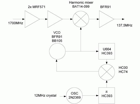
Fig.1. Block diagram of S53MV's converter.
Using PLL if the phase noise is not problem for us can eliminate the disadvantage of the special crystal. Comparison in money is about 10Euro for special Xtal and about 7Euro for PLL & microcontroller. Other problem of PLL is what device type to use. It should work up to about 1.7GHz in ideal case, it should be cheap and easy to buy. I didn't find any in Czech republic . Nice circuits are available in quantities of 100 and more... Easier situation is with PLLs to about 1GHz. I selected UMA1014 from Philips which is not really new, but still very good. I found good source for it in good price. Of course, some TV tuner ICs can be used like TSA5511, TSA5512, SDA3202 etc.
UMA1014 works up to 1.1GHz and can't be used for direct signal synthesis at 1.6GHz (1.7GHz-137.5MHz). At this point, harmonic mixer is a solution for us! This mixer needs local oscillator signal at 1 of what is real needed. In our case 776.75MHz is needed for receiving 1st Meteosat channel at 137.5MHz. In fact it is the same principle like was used in HPMX5001. The disadvantage of this mixer is high noise figure which also depends on level of local oscillator signal. Matjaz measured noise figure of about 10dB. With old bipolar transistors at the converter output it resulted in bad noise figure of the entire original S53MV converter. On the other hand, the realization of the harmonic mixer is very easy – two diodes and two striplines at the PCB.
Today there are a lot of good bipolar or unipolar transistors for 2GHz application at the market. It is good to do little calculations before we start to design the converter. The goal is to determine what amplifiers (transistors or ICs) should be used with goal to achieve low noise figure and good gain. Total noise figure of cascaded system is given by Friiss formula:
NF(system) = NF(1) + (NF(2) - 1) / (A P (1)) + (NF(3) - 1) / (A P (1)A P (2))+ (NF(k) - 1) / (A P (1)A P (2)..A P (k-1))
where NF(x) are noise figures of given stages and Ap(x) are related gains
I wrote short Excel macro for comfortable calculations. We just wrote inputs (noise figure and gain) in dB and we will see total parameters of the system.
The block diagram of our system is shown at Fig.2. The input transistor is followed by band pass filter realized at standard FR4 PCB. The next amplifier stage can be realized by another transistor or by monolithic integrated circuit (MMIC). Next filter is followed by harmonic mixer and easy amplifier at 137.5MHz.
During development stage I was thinking about 3 variants. First one was with old MRF571 transistors; the second was with new bipolar transistors at both stages. The last one was with GaAs FET transistor at the output followed by MMIC amplifier. I chose BFP183 as standard bipolar transistor with guaranteed gain 12dB and NF 2dB at 1.8GHz. ATF21186 was my choice for cheapest GaAs FET I can obtain, gain 13dB ad NF 0.6dB. For MMIC I used non-standard SGA4586 from Sirenza Microdevices with gain 18dB and NF 1.9dB. This is good parameter compared to other MMICs with NF about 4dB. Last amplifier stage is realized with BFR93 (BFR91 in original article). Tables below summarize all these parameters and we can see total noise figure at each system point. Readers can play with XLS file and can see real impact of bad or good transistor at the input or at the output.
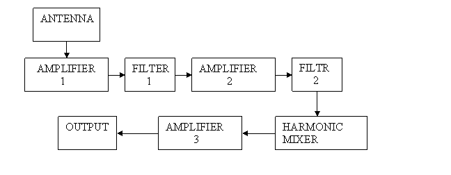
Fig.2. Converter system block diagram.
Tab.1. Original S53MV's schematic.
|
Amp1 |
Filter1 |
Amp2 |
Filter2 |
Mixer |
Amp3 |
Noise figure [dB] |
4 |
3 |
4 |
3 |
10 |
3 |
Gain [dB] |
7 |
-3 |
7 |
-3 |
-10 |
15 |
Noise figure |
2.51 |
2.00 |
2.51 |
2.00 |
10.00 |
2.00 |
Gain |
5.01 |
0.50 |
5.01 |
0.50 |
0.10 |
31.62 |
NF total |
2.51 |
2.71 |
3.31 |
3.39 |
4.82 |
6.40 |
NF total [dB] |
4.00 |
4.33 |
5.20 |
5.30 |
6.83 |
8.06 |
Gain total [dB] |
7 |
4 |
11 |
8 |
-2 |
13 |
Tab.2. Version with BFP183 at both amplifier stages.
|
Amp1 |
Filter1 |
Amp2 |
Filter2 |
Mixer |
Amp3 |
Noise figure [dB] |
2 |
3 |
2 |
3 |
10 |
1.2 |
Gain [dB] |
12 |
-3 |
12 |
-3 |
-10 |
20 |
Noise figure |
1.58 |
2.00 |
1.58 |
2.00 |
10.00 |
1.32 |
Gain |
15.85 |
0.50 |
15.85 |
0.50 |
0.10 |
100.00 |
NF total |
1.58 |
1.65 |
1.72 |
1.73 |
1.87 |
1.92 |
NF total [dB] |
2.00 |
2.17 |
2.36 |
2.38 |
2.72 |
2.84 |
Gain total [dB] |
12 |
9 |
21 |
18 |
8 |
28 |
Tab.3. Version with ATF21186 and SGA4586
|
Amp1 |
Filter1 |
Amp2 |
Filter2 |
Mixer |
Amp3 |
Noise figure [dB] |
0.6 |
3 |
1.9 |
3 |
10 |
1.2 |
Gain [dB] |
13 |
-3 |
18 |
-3 |
-10 |
20 |
Noise figure |
1.15 |
2.00 |
1.55 |
2.00 |
10.00 |
1.32 |
Gain |
19.95 |
0.50 |
63.10 |
0.50 |
0.10 |
100.00 |
NF total |
1.15 |
1.20 |
1.25 |
1.25 |
1.28 |
1.29 |
NF total [dB] |
0.60 |
0.78 |
0.98 |
0.98 |
1.08 |
1.12 |
Gain total [dB] |
13 |
10 |
28 |
25 |
15 |
35 |
I decided to realize version from Tab.3. because I had good experiences from my previous design. The goal was to achieve noise figure at about 1dB and enable users to use the converter with small dish and without pre-amplifier.
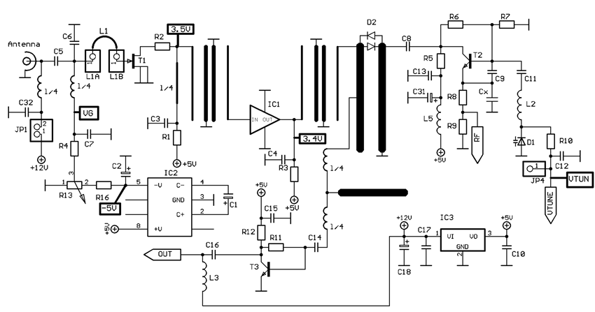
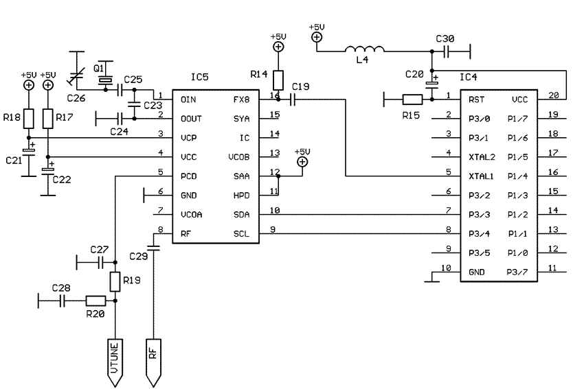
Fig.3. Converter schematic.
Overall converter schematic is shown in Fig.3. L1 and C6 forms easy matching circuit for optimum noise figure of the T1. T1 is connected with grounded source. It includes negative bias voltage at the gate but the main advantage is very good stability. IC2 (ICL7660) is +5V to –5V converter, R13 is used for adjusting the best gain and NF at the T1. R2 in its drain improves stabilization and makes loading together with filter F1 (band pass 1.7GHz). This filter is realized by 2 lambda/4 resonators with coupling lines at standard FR4 PCB material. T1 drain is connected to +5V power supply via R1 and lambda/4 coil realized also at PCB. IC1 is monolithic amplifier (MMIC) SGA4586, R3 and C4 are biasing components. R3 determines amplifier current, it is 45mA as is recommended in the datasheet. You can use different type of the IC1 but you need to change value of the R3. You can also change T1 but you need to modify R1, R2 and sometimes also L1 and C6. Be careful, new transistors have VDS max 2V! Harmonic mixer with D2 and D3 is connected behind the next filter. The principle is shown in the Fig.4.
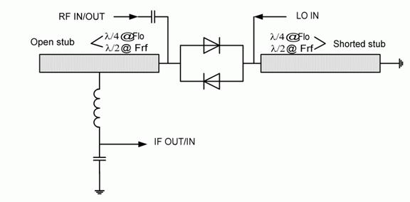
Fig.4. Harmonic mixer realization.
The frequency of the oscillator with T2 (BFR93) is determined by L2 and capacity of D1. C9 and Cx are capacitance divider, Cx is realized on PCB. Signal for PLL is taken from emitter divider R8, R9. L5, C31 and C13 make Vcc filtration. L2 is realized from piece of 0.8mm CuAg wire formed to „U“ with dimensions 10x5mm.
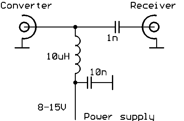
Final signal from the mixer is filtered in L6, L7 and open stub and boosted in IF amplifier with T3 (BFR93). The output signal is connected to the connector via C16 which separates DC component. Power supply for the converter is connected via cable and is separated by L3. IC3 (MC7805) provides power supply stabilization. Most of receivers enable to bias the converter or preamplifier via cable. If you want use scanner or TRX without this option, you can build simple biasing interface, see Fig.14. L8, C32 and JP1 at converter PCB enables to bias 1.7GHz preamplifier. If you need 5V for preamp, simply cut PCB track and connect it to +5V.
Digital part of the converter includes PLL synthesizer IC5 (UMA1014) in standard application. Reference quartz Q1 (8MHz) stability determines stability of the entire converter. Its frequency can be slightly adjusted by C26. Microcontroller IC4 (AT89C2051) sends data to the PLL. Its timing is derived from FX8 pin of IC5 where signal from reference oscillator divided by 8 is available. So with quartz 8MHz we have 1MHz signal for the microcontroller. The function of the controller is very easy. It sends data to the PLL and goes to sleep mode. Sleep mode reduces possible interferences. You can change frequency of the oscillator to 778.25MHz by shorting P3.7 to the GND. This frequency is needed if you want to receive Meteosat's channel2 at 137.5MHz.
Program itself is very easy. It sets all registers in UMA1014. Registers determine PLL parameters and main divider value. In this application reference crystal 8MHz is used, so for 50kHz step we need:
Nref = 8000000/50000 = 160
This value is available in UMA1014 at code (0001b) for bits A3-A0, see datasheet.
The oscillator frequency for input signal 1691MHz, the output at 137.5MHz is:
Fosc = (1691 – 137.5) / 2 = 776.75MHz
With step 50kHz we calculate value for main divider as:
Nmain = 776750000 / 50000 = 15535 (3CAFh)
Some other functions have to be set:
110001 0 0 b – device address , SAA pin at +5V , write
111 1 1 0 00 b – disable alarm , auto-increment , following register A
0 0 0 1 0001 b – no power down , current 0.5mA , reference divider 160
101 0 01 00b – passive filter , VCO A
00111100b – main divider, high byte
10101111b – main divider, low byte
All the program (without I2C routines):
org 00h
jmp START
org 20h
START:
mov FREQL,#0AFh
mov FREQH,#3Ch
call IISTART
mov A,#11000100b
call IIWR
mov A,#11111000b
call IIWR
mov A,#00010001b
call IIWR
mov A,#10100100b
call IIWR
mov A,FREQH
call IIWR
mov A,FREQL
call IIWR
call IISTOP
mov IE,#81h
mov 87h,#01 ; IDLE
nop
jmp START
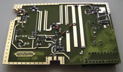
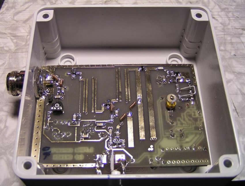
The converter is realized on double side PCB with through holes at 0.8mm FR4 material. RF circuits are placed on one side, PLL and microcontroller on the second side. The input connector is N-type female, the output one can be either BNC or F. The entire converter is housed in waterproof box LUCA with dimensions 110x110x58mm.
Coils marked as „l/4“ are quarter-wave choking coils from 6cm of 0.15mm Cu enameled wire. Solder wire ends 5mm at each side and turn it to 1mm diameter (drill). Coil detail is visible at Fig.5. L1 is piece of 0.6mm CuAg wire bended to the PCB, see fig.8.
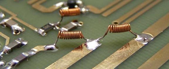
Fig.5. Detail of quarter wave coil.
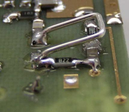
Fig.6. Detail of the L2.
Most of the components are SMD, 1206 size. You haven't to worry about soldering, there is enough space around. Fig.7. shows packages of not not standard components.
Fig.7. Packages of not standard components.
Assembly and debugging
In the beginning visual inspection of the PCB is recommended. At first all components of the oscillator and PLL should be assembled. You don't need socket for the microcontroller Connect external power supply +5V and check tunning voltage at VTUN point. If PLL is in lock, VTUN must be between 0-5V and will respond if you move your finger near L2. The optimal value should be 2.5V. If it is not your case, deform L2 little bit. If you compress „U“, voltage will go up and vice-versa. If the tunning voltage is at upper limit, the oscillator frequency is too low and you need to shorten L2. Otherwise if VTUN is too low, you need to decrease oscillator's frequency. Fine tunning can be done also by adding solder to L2 pins.
If you have some scanner, it is very good helper as you can here if the signal is clear, without any parasitic modulation. Usualy DC-DC converter ICL7660 can make some acoustic noise or some oscillating amplifier.
L2 details are shown in the Fig.8. If you still can't put PLL to the lock, you will need an counter and check 1MHz signal at pin 16 of IC5 and also exact frequency of the oscillator with L2.
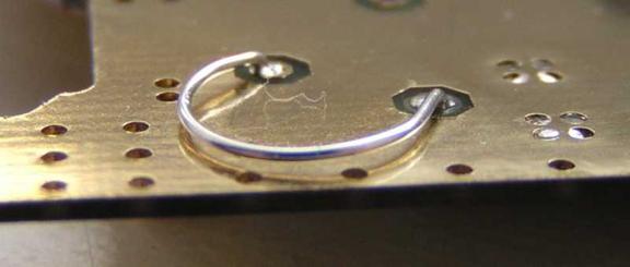
Fig.8. L1 detail.
All remaining components without T1 and IC1 can be assembled in next phase. Check correct function of the IC2 and set VG voltage to –0.8V by R13. Also check voltages at R2 and R3. If everything is ok, disconnect power supply and connect IC1. Then you can also carefully solder T1. Remember that T1 is very sensitive device and make sure you will not destroy it by electrostatic discharge. Never touch the gate. Now again check voltages at R2 and R3 and compare it with values in the schematic. Once you solder T1, don't power converter without any load at the input. Use 50 ohm resistor instead of real antenna.
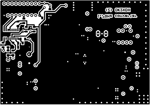
Fig.9. PCB drawing, bottom.
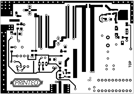
Fig.10. PCB drawing, top.
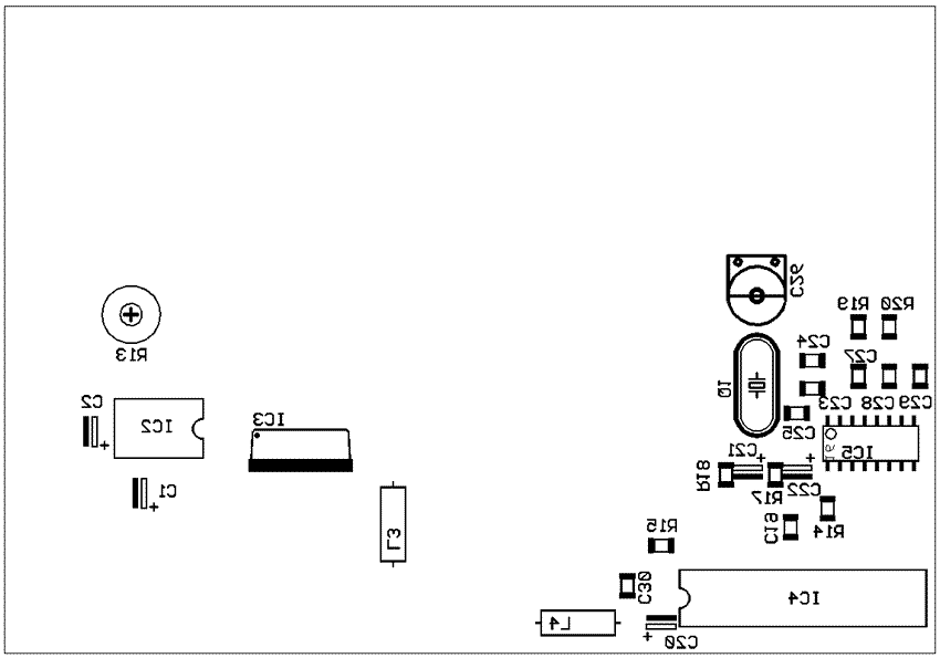
Fig.11. Assembly diagram, bottom.
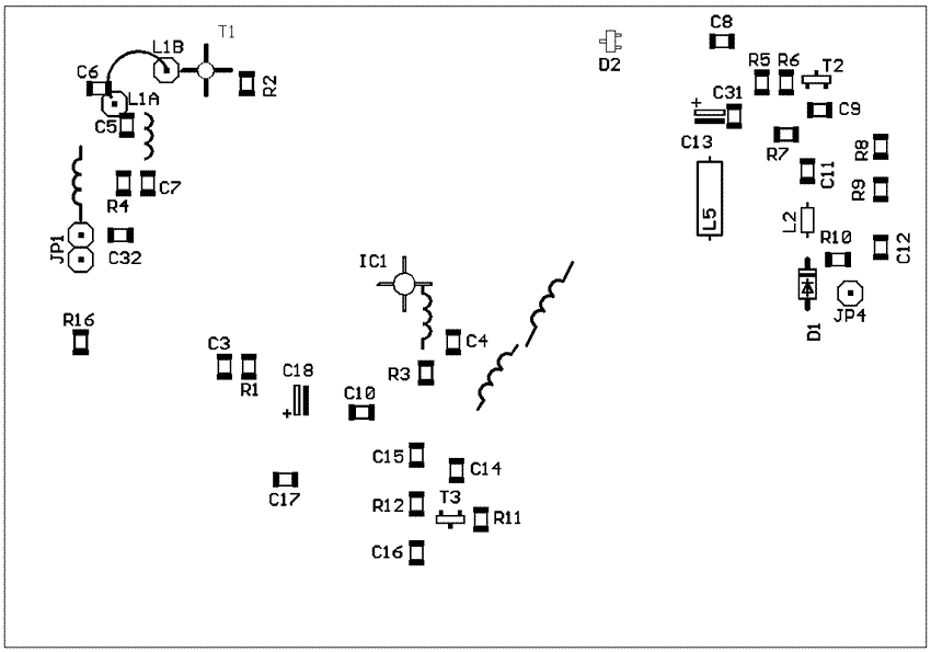
Fig.12. Assembly diagram, top.
Obr.14. Biasing through the cable.
For final tuning you need to connect the converter to real antenna pointed to the satellite or to the signal generator. I'm using 60cm dish in room pointed to Meteosat through the window. If the converter works ok you have to hear the signal now. Use R13 for achieving the best signal purity. Exact converter frequency can be tuned by C26.
If you use the converter in environment with big temperature changes, crystal heating is recommended. The best way is to use PTC thermistor or some method described for microwave radio amateur constructions.
Conclusions
Described converter shows that it is not problem to make construction working at 2GHz at low cost today. No special instruments are needed for the converter debugging. Thanks to good components, low noise figure and high gain is not problem even for amateur constructions.
The converter haven't to be used for Meteosat only. I want to try it for NOAA HRPT receiving. With small change of used filters it can be used for Inmarsat monitoring (A-type terminals).
The advantage of this construction is that components can be simply replaced by other types. IC1, T1 and D2 can be taken from old satellite tuners. PLL IC can be replaced by other circuits from TV tuners etc..
Used components:
C1,2,18,21,22,31 33u/16V
C3,4,7,12,13,15,32 1n
C5,14,16,25 100p
C6 1p8
C8 1p5
C9 1p
C10,17,19,30 100n
C11 12p
C20 10u
C23 68p
C24,24 39p
C27 2n2
C28 180n
C26 15p trimmer Philips
D1 BB221
D2 MMD353LT1
IC1 SGA4586
IC2 ICL7660
IC3 MC7805T
IC4 AT89C2051
IC5 UMA1014
L1 see text
L2 see text
L3,5 10u
L4 100u
Q1 8MHz
R1,4 47
R2,12 12
R3 33
R5,12,17 68
R6,10,15 8k2
R7,19 18k
R8 180
R9 56
R11 4k7
R14,20 10k
R13 10k trimmer
R16 33k
T1 ATF-21186
T2,3 BFR93

|